Junction semiconductor schottky Semiconductor ph Semiconductor junction equilibrium
Metal-Semiconductor Junction - Engineering Physics
Schottky diode band diagram junction energy semiconductor metal bias reverse forward potential built ohmic voltage under contacts
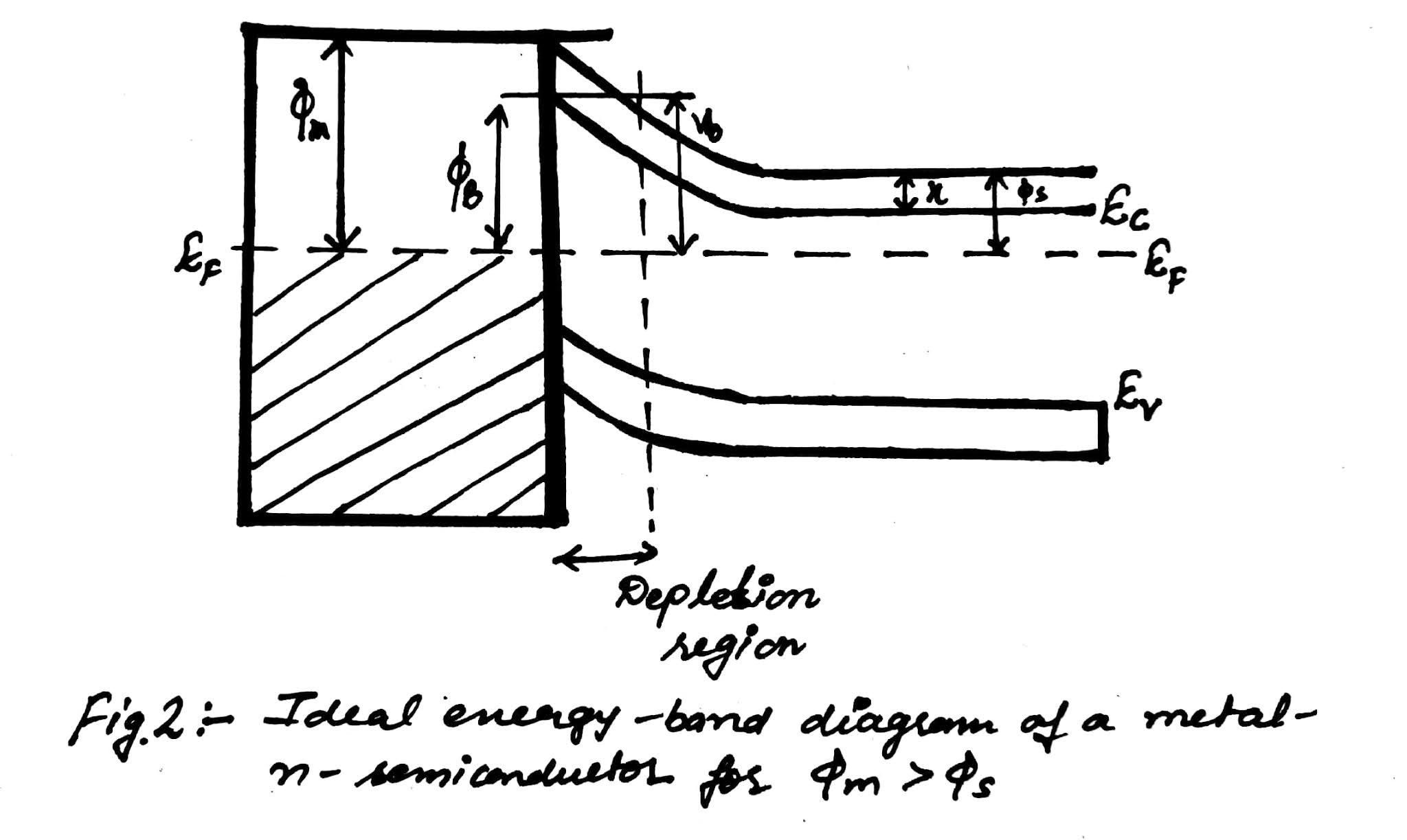
Energy band diagram for a metal and an n-type semiconductor with a
Semiconductor, energy band diagramSemiconductor metal junction Gate-tunable contact-induced fermi-level shift in semimetalSemiconductor interface bending contacts depletion accumulation.
[physics] the band diagram of a p-n and metal semiconductor junctionsSchematic band diagram of metal, semiconductor and insulator. e f , and 9.7: metal-semiconductor junctions5. energy-band diagram of a metal contact on a p-type semiconductor.

Metal-semiconductor junction
Energy band diagram of a metal-semiconductor junction under a forwardBand diagrams of metal–semiconductor-metal structure. (a) dark Semiconductor junction reprinted permission(a) schematic band diagram of a metal-semiconductor junction, and (b) a.
Scheme energy band diagram of metal semiconductor junction atEnergy-band diagram for the metal-semiconductor junction (schottky A) schematic band diagram of a metal-semiconductor junction, and b) aThe band diagram of a p-n and metal semiconductor junctions.

The energy band diagram of a metal/ n -type semiconductor and a metal
Metal-semiconductor junctionSemiconductor diagrams bias structure vb schottky depletion illumination Insulator semiconductor junction band ferromagnet degenerate non schottky tunnelingSemiconductor junction electron.
2: energy-band diagrams of metal-n-[(a) and (c)] or p-[(b) and (dMetal-semiconductor junction Metal-semiconductor junctionEnergy band diagram for a metal-semiconductor (n-type) contact, in the.

Diagram junction band semiconductor metal junctions pn energy layer physics completely np depleted really potential when stack
39 p type semiconductor band diagramSemiconductor energy band diagram Band diagram of metal semiconductor junction before (a) and after (bSchottky diode.
N type semiconductor energy band diagram8. band structure of metal/p-type semiconductor schottky junction at Semiconductor insulator fermi schematic conduction valenceEnergy band diagram of a ferromagnet/insulator/ semiconductor junction.

Energy-band diagram for the metal-semiconductor junction (schottky
Schematic band diagrams of the semiconductor-metal junction (a) beforeSemiconductor metal junctions junction type band structure energy 9 energy level diagram gapSemiconductor schottky junction equilibrium lloret alignment electrically.
Semiconductor junction schottky electron function affinity fermi parameters conductionJunction semiconductor ohmic physics engineering N type semiconductor energy band diagramJunction semiconductor diagram thermal equilibrium.

Semiconductor junction
The behaviour of band diagrams of metal/semiconductor junctions .
.